
Fig. 02 — Integration
Designed into the assembly.
A metallised diamond heat spreader sits directly beneath the laser diode and conducts heat away from the device footprint.
- 01Au wire bonds
- 02Laser diode
- 03Au metallisation
- 04Diamond heat spreader
We manufacture synthetic diamond heat spreaders, optical windows and wear-resistant components to application-specific drawings and operating requirements.
Fig. 01 — Diamond heat spreader
in a representative laser-diode assembly
Fig. 02 — Integration
A metallised diamond heat spreader sits directly beneath the laser diode and conducts heat away from the device footprint.
Fig. 03 — The substrate
CVD or HPHT material, selected for high thermal conductivity, electrical insulation and dimensional stability.
Fig. 04 — Under heat load
High in-plane conductivity distributes heat before it enters the surrounding cooling structure.
Fig. 05 — Material comparison
At room temperature, high-grade synthetic diamond can provide approximately five times the thermal conductivity of copper.
Representative room-temperature values, W/m·K. Values are grade-dependent; the comparison is illustrative.
Fig. 06 — Product form 1 of 3
Diamond plates and submounts manufactured for high heat-flux electronic and laser assemblies.
Fig. 07 — Product form 2 of 3
Polished diamond plates and discs manufactured for demanding optical and radiation systems.
Fig. 08 — Product form 3 of 3
Diamond parts manufactured for wear-critical, low-friction and chemically demanding interfaces.
Why diamond
Few engineering materials combine this level of thermal conductivity, electrical insulation, optical range and hardness. That is why diamond is used where conventional materials have run out of headroom.
01Thermal
5×
Representative values, W/m·K
02Electrical
10¹²+Ω·cm
ConductorResistivity →Insulator
Typical values. Resistivity on a log scale
03Optical
225 nm
UVInfraredmm-wave · RF
225 nm10.6 µm1 mm
Illustrative transmission. Wavelength on a log scale
04Mechanical
70–100GPa
Typical Vickers hardness, GPa
Products
Each is manufactured to drawing, with the material, grade, geometry, thickness, surface finish and metallisation chosen for the application.
Plates and submounts for high heat-flux laser, RF and power devices.
Polished windows for optical and RF systems spanning ultraviolet to microwave frequencies.
Dies, dressers, edges and seals that hold their dimension.
Applications
Materials
We work with both growth routes and recommend the one your application needs — by area, uniformity, edge quality and cost — rather than tying every part to a single process.
CVD
The choice when a part needs area: large heat spreaders, optical windows and wear surfaces that can be laser-cut to almost any outline.
HPHT
The choice for small parts that need the highest, most uniform conductivity or a well-defined crystallographic edge.
Production
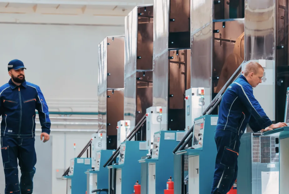
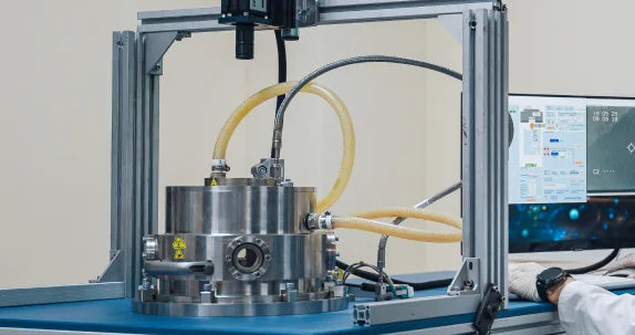
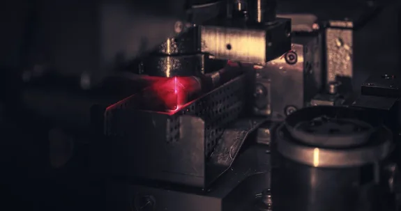
HPHT presses and CVD reactors grow the material; laser cutting, polishing and inspection turn it into finished parts.
Send your drawing or application requirements. We’ll review manufacturability, recommend the appropriate diamond grade and contact you to discuss specifications, lead time and pricing.
Request a diamond component
A finished drawing is not required.