CVD and HPHT diamond

The two material forms we supply each have distinct strengths. We select the growth route and grade for every part based on its application requirements.

CVD wafer · up to Ø 100 mmHPHT crystal · up to 8 × 8 mm
Thermal conductivity
Up to 2,200 W/m·K
CVD wafers
Up to Ø 100 mm
HPHT plates
Up to 8 × 8 mm
Material options
7 listed below

Growth routes

How each one is made, and what it is for.

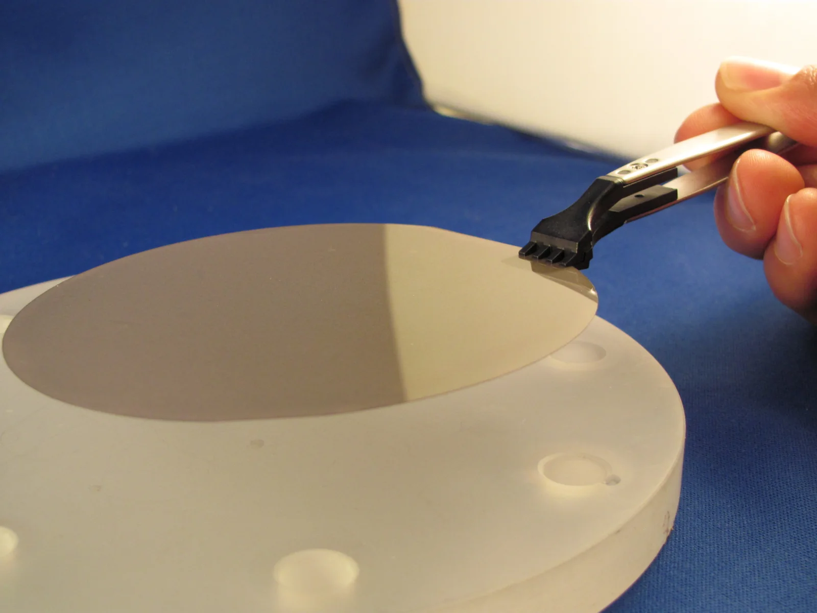
A polished CVD polycrystalline diamond wafer lifted from its holder with tweezers

CVD polycrystalline

Deposited layer by layer from a carbon-bearing gas in a plasma reactor, then separated from the growth substrate to produce free-standing wafers up to Ø 100 mm.

The choice when a part needs area: large heat spreaders, optical windows and wear surfaces that can be laser-cut to almost any outline.

Thermal conductivity
1,000–2,000 W/m·K
Wafer size
Up to Ø 100 mm
Thickness
0.1–2.0 mm

Best for

  1. 01Heat spreaders above a few millimetres
  2. 02Optical and microwave windows
  3. 03Large wear surfaces
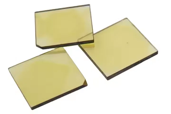
Three yellow HPHT single-crystal diamond plates

HPHT single crystal

Grown from a metal solvent at high pressure and temperature, the conditions under which natural diamond forms.

The choice for small parts that need the highest, most uniform conductivity or a well-defined crystallographic edge.

Thermal conductivity
Up to 2,200 W/m·K
Plate size
Up to 8 × 8 mm
Grain boundaries
None

Best for

  1. 01Submounts under single emitters
  2. 02Precision cutting edges
  3. 03Small precision wear parts

Comparison

Side by side.

CVD polycrystallineHPHT single crystal
StructurePolycrystalline, columnar grainsSingle crystal
Thermal conductivity1,000–2,000 W/m·K by gradeUp to 2,200 W/m·K
Largest partØ 100 mm waferAbout 8 × 8 mm plate
Optical useOptical grades for UV, visible, IR and RF applicationsType IIa for optics; Type Ib is yellow
Edge qualityLaser-cut, limited by grain sizeCrystal edge, can be sharpened
CostLowest per area for large partsLowest for small precision parts

Grades

Standard material options.

Thermal grades are named by their minimum room-temperature conductivity. Optical, mechanical and other material options are selected by application.

GradeMaterialKey valueTypical use
Thermal 1000CVD≥ 1,000 W/m·KPower modules, cost-sensitive spreaders
Thermal 1500CVD≥ 1,500 W/m·KGaN RF amplifiers, laser bars
Thermal 1800CVD≥ 1,800 W/m·KHigh heat-flux laser diodes
Thermal 2000CVD≥ 2,000 W/m·KHighest heat-flux devices
Single crystalHPHTUp to 2,200 W/m·KSingle-emitter submounts, precision parts
OpticalCVD< 0.07 cm⁻¹ at 10.6 µmCO₂ laser and IR windows
MechanicalCVD / HPHT70–100 GPa hardnessWear parts and tooling

Representative values. The final specification is confirmed in the quotation.

Reference

Properties of diamond.

Representative intrinsic values at room temperature for the early design calculations that come before a finished drawing.

Density
3.52g/cm³
Young's modulus
1,050GPa
Hardness
70–100GPa
Thermal expansion
1.0ppm/K at 300 K
Band gap
5.47eV
Refractive index
2.41visible; 2.38 at 10.6 µm
Electrical resistivity
≥ 10¹²Ω·cm, grade-dependent
Dielectric constant
5.7

Not sure which grade fits?

Send the application and the operating conditions. We’ll recommend CVD or HPHT and the grade that meets the requirement at the lowest cost.

Contact and FAQ