
From drawing to finished part
Material selection, cutting, finishing, metallisation and inspection, handled under one specification and one point of contact.
- Thickness
- 0.1–2.0 mm, ±0.05
- Polished surface
- Ra < 20 nm
- Flatness
- < 10 µm over 25 mm
- Largest part
- Ø 100 mm
Process
Five steps, one specification.
- 01
Review
We read your drawing or requirements — heat load, optical band, wear conditions — and confirm what can be made.
- 02
Material
We recommend CVD or HPHT and the grade that meets the requirement at the lowest cost.
- 03
Cutting
Plates and crystals are laser-cut to the outline on the drawing.
- 04
Finishing
We lap, polish and metallise parts to the specified thickness, surface finish and metal stack.
- 05
Inspection
Each batch is checked for dimensions, flatness and surface before it ships.
Production
Grown and finished under one roof.
HPHT presses and CVD reactors grow the material; laser cutting, polishing and inspection turn it into finished parts.

01HPHT
Powder preparation
Powder mixtures for the growth cell are prepared to the recipe for each target crystal.
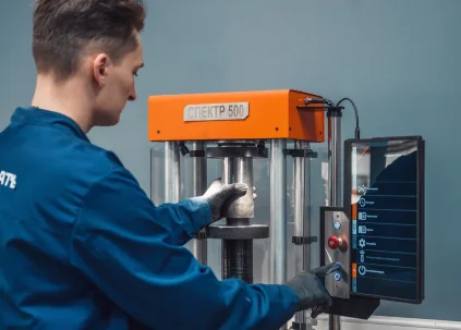
02HPHT
Cell pressing
Growth-cell parts are pressed and machined on our own equipment.
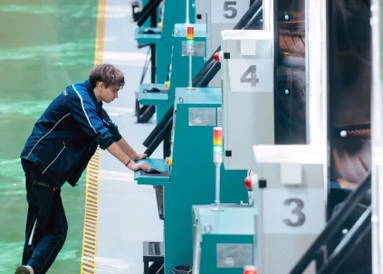
03HPHT
HPHT synthesis
Single crystals grow in latest-generation cubic presses, then are cleaned out of the cell.
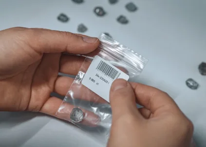
04HPHT
Sorting
Grown crystals are sorted, labelled and tracked by batch.
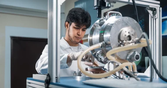
05CVD
Reactor preparation
Substrates and the reactor chamber are prepared for each growth run.
06CVD
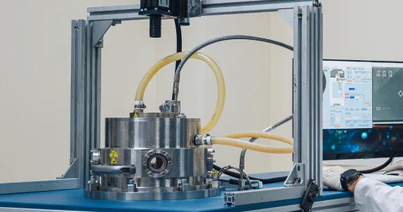
CVD growth
Microwave plasma reactors grow polycrystalline and single-crystal diamond.
07Finishing
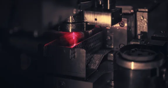
Laser cutting
Precision laser systems cut plates and crystals to the outline on the drawing.
08Finishing
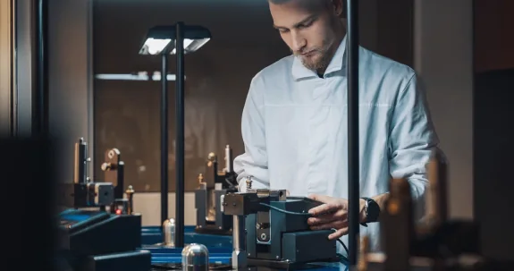
Polishing
Plates are lapped and polished on manual and automatic machines.
09Finishing
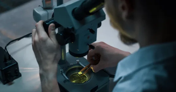
Inspection
Crystals, plates and substrates are checked under a polarising microscope.
Processing
Tolerances and finishes.
Typical values for standard work. Tighter tolerances are quoted per project.
- Thickness
- 0.1–2.0 mm±0.05 mm
- Outline
- Laser-cut to drawing+0.1 / −0 mm
- Surface
- As-grown, lapped, polishedRa < 20 nm polished
- Flatness
- < 10 µmOver 25 mm
- Parallelism
- < 5 arcminOptical parts
- Metallisation
- Ti/Pt/Au, Ti/Au, Cr/AuAuSn pre-solder
Metallisation
Ready to solder.
Heat spreaders and submounts can be supplied metallised and pre-soldered, so they go straight into die attach.
| Stack | Typical layers | Used for |
|---|---|---|
| Ti / Pt / Au | 0.05–0.1 / 0.1–0.2 / 0.5–3 µm | Standard for AuSn die attach; Pt blocks solder diffusion |
| Ti / Au | 0.05–0.1 / 0.5–3 µm | Wire bonding and general soldering |
| Cr / Au | 0.05–0.1 / 0.5–3 µm | Alternative adhesion layer |
| AuSn 80/20 | 2–8 µm | Pre-deposited solder for fluxless die attach |
Quality
Checked before it ships.
Every batch is inspected against the drawing. Prototype quantities for qualification and recurring production volumes follow the same process.
- 01Dimensions and thickness
- 02Flatness and parallelism
- 03Surface roughness
- 04Visual inspection for chips and cracks
- 05Metallisation adhesion
- 06Thermal conductivity data on request
Have a drawing or a heat problem?
Send your drawing or operating requirements. We’ll review manufacturability, recommend the diamond grade and reply with specifications, lead time and pricing.